WEBINAR | Up to 40% Faster Automated TEM Lamella Preparation with new Ga⁺ FIB Column

Deliver Smooth, Controlled Delayering for Faster Defect Localization

Modern semiconductor failure analysis demands delayering that is fast and precise, while also protecting delicate structures. TESCAN workflows create smooth, uniform surfaces, stop exactly at the target layer, and preserve integrity for immediate, reliable analysis.

Prepare samples for defect localization or in-situ electrical testing, cleanly and efficiently, across sub-20 nm nodes and complex I/O stacks.

Group 658
Frame 915

Tescan solutions

FOR THE WHOLE SEMINCONDUCTOR RESEARVCH AND PRODUCTION PROCESS
Delayering Sub-20 nm Nodes

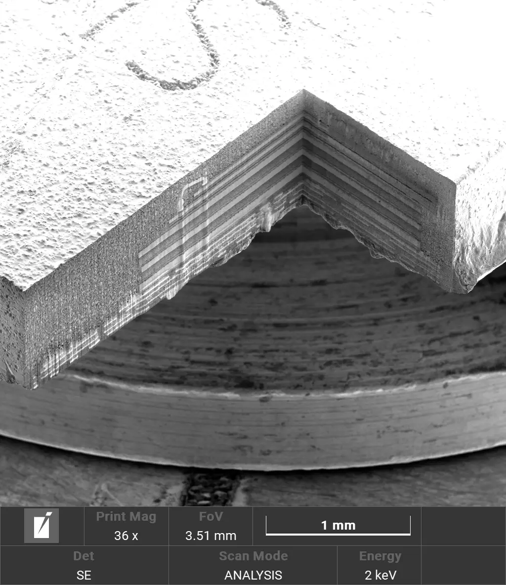
Use an integrated plasma FIB workflow with precise endpoint control and in-situ nanoprobing to achieve clean, planar delayering of sub-20 nm semiconductor nodes. This approach preserves structural integrity and prepares samples for immediate electrical and structural analysis.

  • Uniform layer removal: Prevents damage to delicate metals and dielectrics
  • Real-time endpoint monitoring: Ensures accurate layer targeting
  • In-situ probing: Enables direct electrical testing without sample transfer
Low Angle Polishing for Delayering of Thick Upper Layers

Combine femtosecond laser ablation for rapid material removal with precision Xe plasma FIB polishing to enable fast, accurate, low-damage failure analysis of large and complex semiconductor devices. This hybrid workflow improves throughput and preserves critical structures, from package to nanoscale.

  • Laser ablation: Quickly removes bulk material without mechanical stress or overheating
  • Plasma FIB: Low angle polishing ensures uniform material removal across the I/O area.Integrated overlays and CAD alignment: Ensure accurate targeting across tools and samples
2_Low Angle Polishing FIB milling strategy_1x

Tescan Solutions

for Delayering and Failure Analysis

Tescan AMBER X – Plasma FIB-SEM for Multimodal Battery Analysis

TESCAN AMBER X gives you the tools to study battery electrodes, from nanoscale interfaces to bulk. SEM imaging, plasma FIB milling, and chemical analysis in one workflow let you track degradation and perform 3D reconstructions with precise, repeatable results.

  • BrightBeam™ SEM: High-resolution, low-kV imaging of sensitive electrode surfaces
  • iFIB+™ Xe plasma source (3–30 keV): Fast, precise milling for large-area or site-specific analysis
  • Integrated analytical tools (EDS, EBSD, ToF-SIMS): Correlate structure and chemical composition in a single system
  • Endpointing and delayering workflows: Ensure accurate targeting of buried features
  • In-situ nanoprobing: Enable direct electrical characterization without sample transfer


Tescan Essence™ with Low Angle Polishing Module

TESCAN Essence™ automates plasma FIB delayering for thick-layer semiconductor analysis. Shallow-angle exposure and live BSE monitoring give you controlled removal of upper metal layers and complex chip regions with precision and consistency.

  • Four-direction polishing: Produces curtaining-free surfaces
  • In-column BSE detection: Provides real-time layer-by-layer tracking
  • Application-tuned design: Enables accurate deprocessing of I/O and passivation layers

Sign up for a personal virtual demo

Our global team is available to answer questions about Tescan solutions for Semiconductors.

GET IN Touch

Contact us

map

Your nearest office is:

Tescan Brno
Libušina tř. 21
623 00 Brno - Kohoutovice

Czech Republic

+420 530 353 411
info@Tescan.com