.webp?hsLang=en)
.webp?hsLang=en)


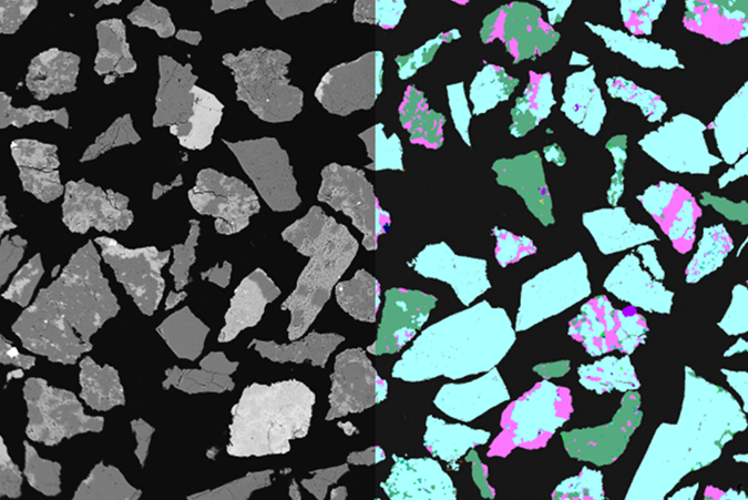
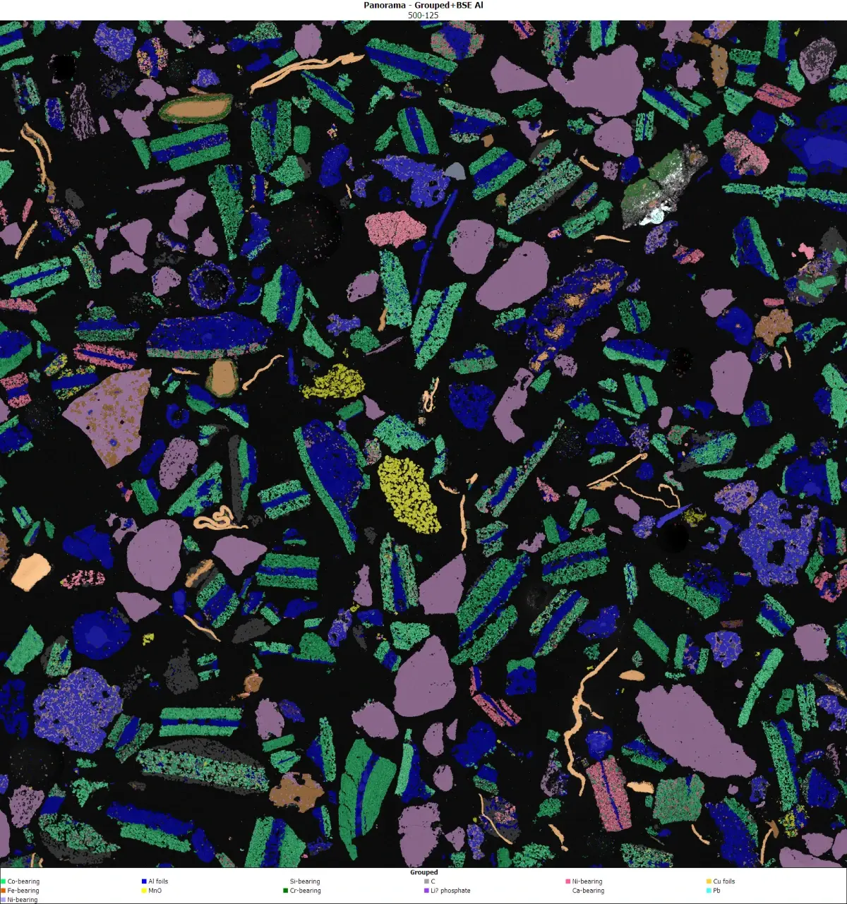
.webp?width=1665&height=1242&name=1_Phase%20map%20of%20heat-treated%20black%20mass%20(1).webp)
TESCAN AMBER X 2
Contextual advertising can be profitable. It can either pay for your hosting and maintenance costs for you website or it can pay for a lot more.

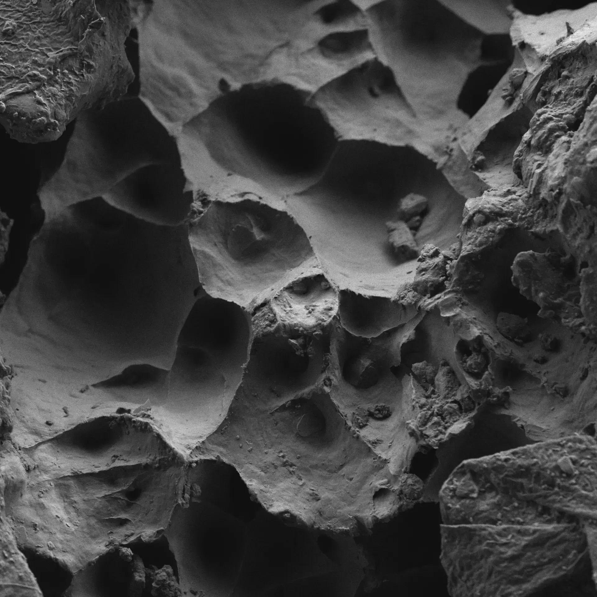
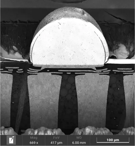
As materials research advances, understanding internal structures, defects, and properties at multiple scales is essential. Tescan’s 3D characterization solutions provide high-resolution insights through micro-CT, FIB-SEM tomography, and correlative imaging, enabling researchers to analyze materials with unmatched precision.


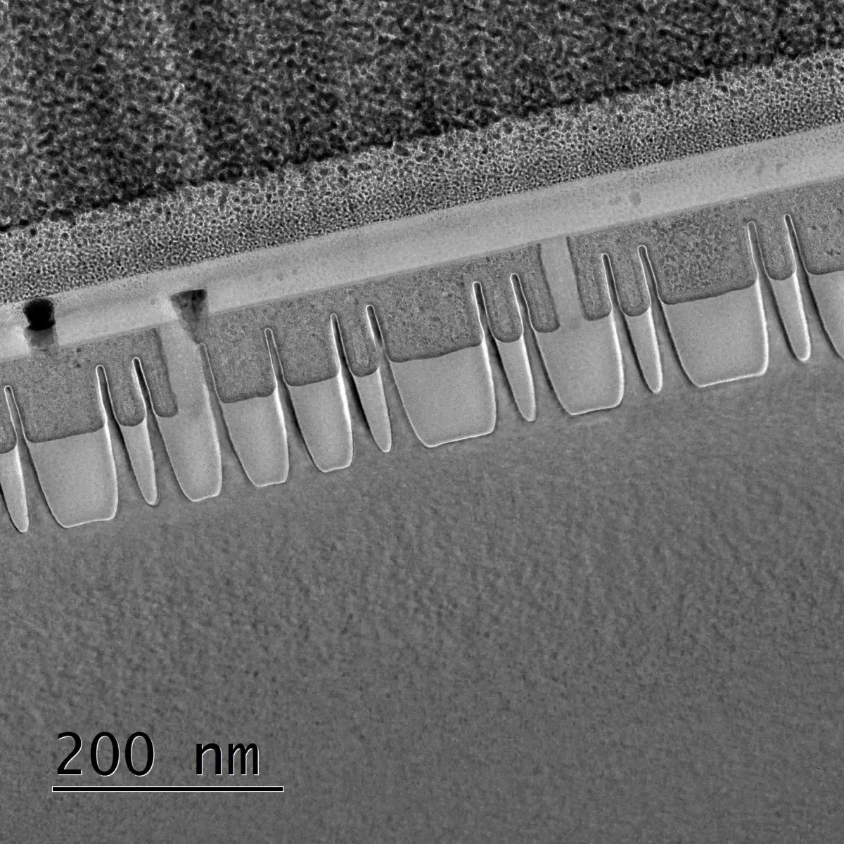
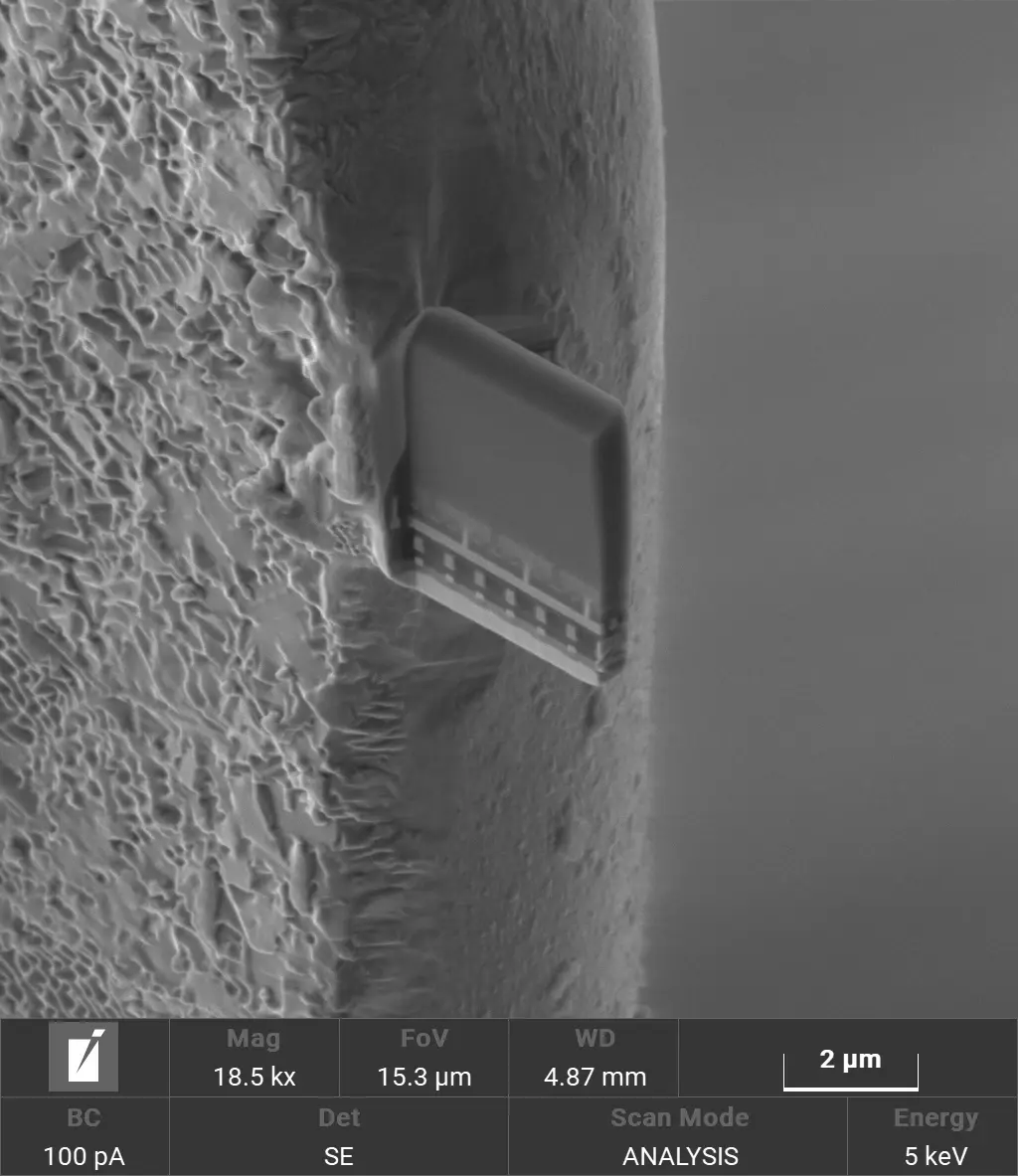
Tescan AMBER X with iFIB+™ control and real-time SE signal end pointing delivers precise Sub-20 nm node delayering. Achieve planar surfaces below 5 nm RMS roughness, maintain dielectric compatibility, and prepare contamination-free structures ready for in-situ nanoprobing and electrical failure analysis.
Tescan AMBER X with iFIB+™ control and real-time SE signal end pointing delivers precise Sub-20 nm node delayering. Achieve planar surfaces below 5 nm RMS roughness, maintain dielectric compatibility, and prepare contamination-free structures ready for in-situ nanoprobing and electrical failure analysis.
.jpg?width=800&height=800&name=Image%20Element%20(1).jpg)
Contextual advertising can be profitable. It can either pay for your hosting and maintenance costs for you website or it can pay for a lot more.
Contextual advertising can be profitable. It can either pay for your hosting and maintenance costs for you website or it can pay for a lot more.

.png?width=400&height=301&name=Image%20Element%20(3).png)
Contextual advertising can be profitable. It can either pay for your hosting and maintenance costs for you website or it can pay for a lot more.
.png?width=400&height=301&name=Image%20Element%20(4).png)
Contextual advertising can be profitable. It can either pay for your hosting and maintenance costs for you website or it can pay for a lot more.
.png?width=350&height=301&name=Image%20Element%20(5).png)
Contextual advertising can be profitable. It can either pay for your hosting and maintenance costs for you website or it can pay for a lot more.
Contextual advertising can be profitable. It can either pay for your hosting and maintenance costs for you website or it can pay for a lot more.
Contextual advertising can be profitable. It can either pay for your hosting and maintenance costs for you website or it can pay for a lot more.
