

Tescan TEM AutoPrep™
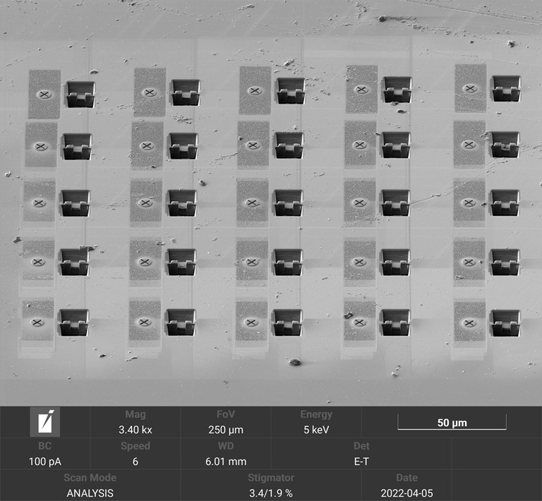
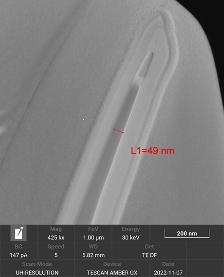
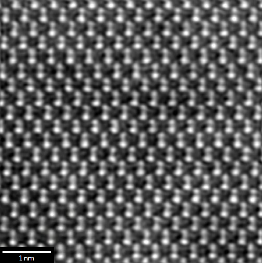
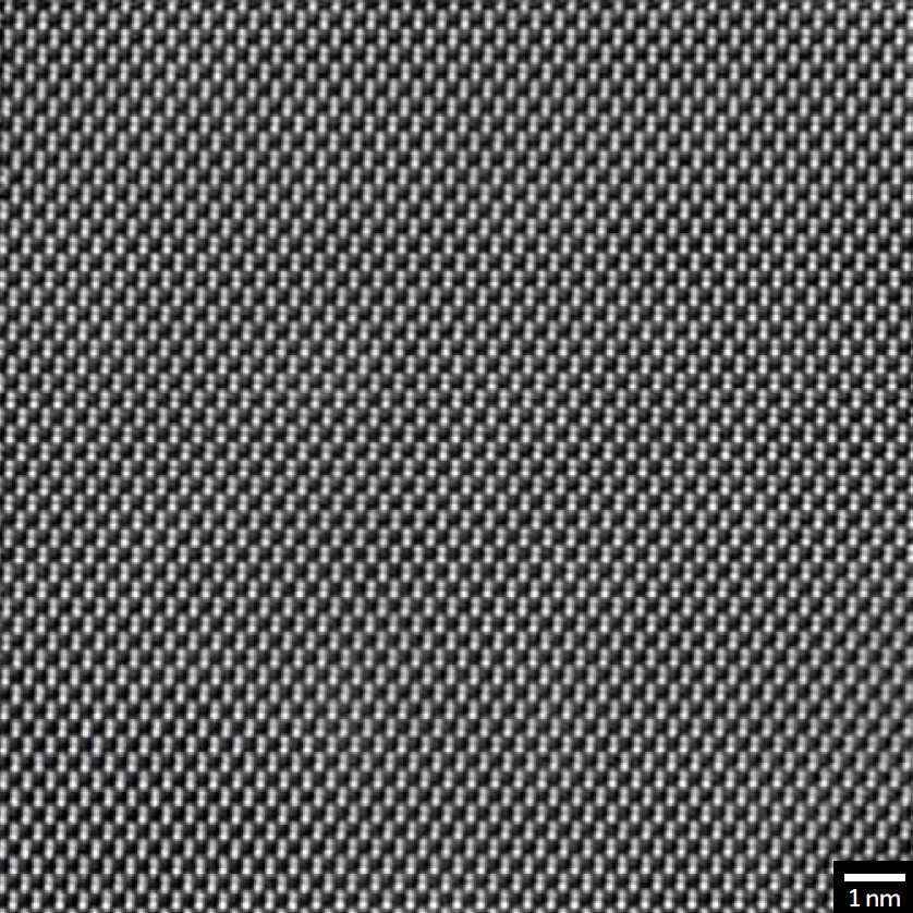
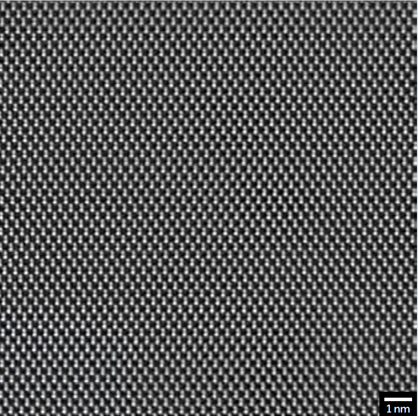
Tescan TEM AutoPrep™ provides automated lift-out, thinning, and polishing workflows for reproducible TEM lamella preparation. In this workflow, it was used to prepare site-specific silicon lamella below 50 nm with accurate [110] orientation for atomic-resolution imaging.
- Automated lamella preparation: Reduces operator dependence and improves reproducibility
- Site-specific lift-out: Ensures correct region and orientation are selected for TEM studies
- Low-kV final polishing: Minimizes amorphous damage and curtaining artifacts
- Workflow integration: Delivers TEM-ready samples directly within the FIB-SEM

.webp?width=229&height=175&name=image3-33-1%20(6).webp)

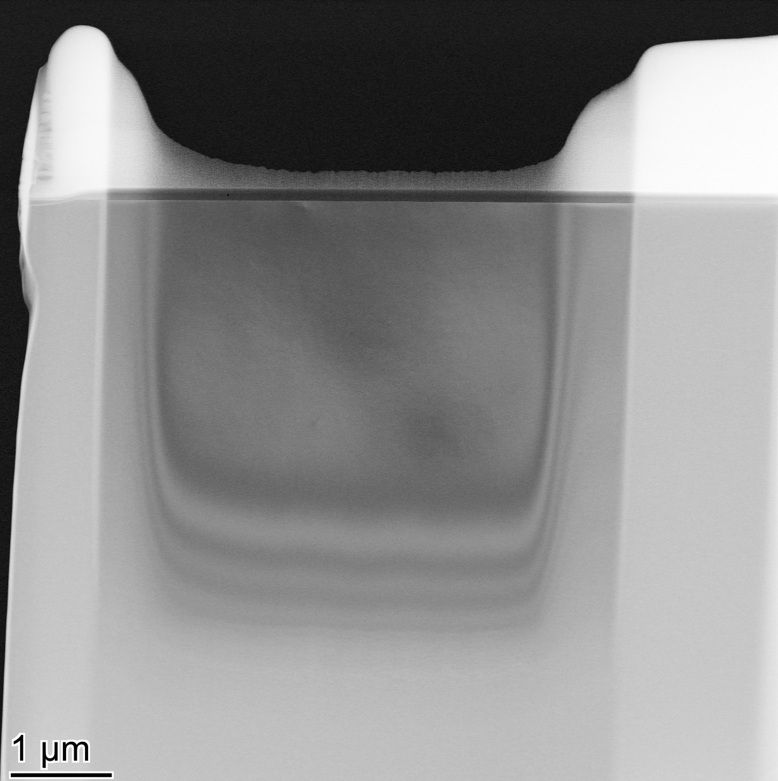
%20lamella%20prepared%20in%20trench%20after%20undercut-1.png?width=1070&height=1004&name=Large%20(55%20um%20x%2030%20um)%20lamella%20prepared%20in%20trench%20after%20undercut-1.png)
