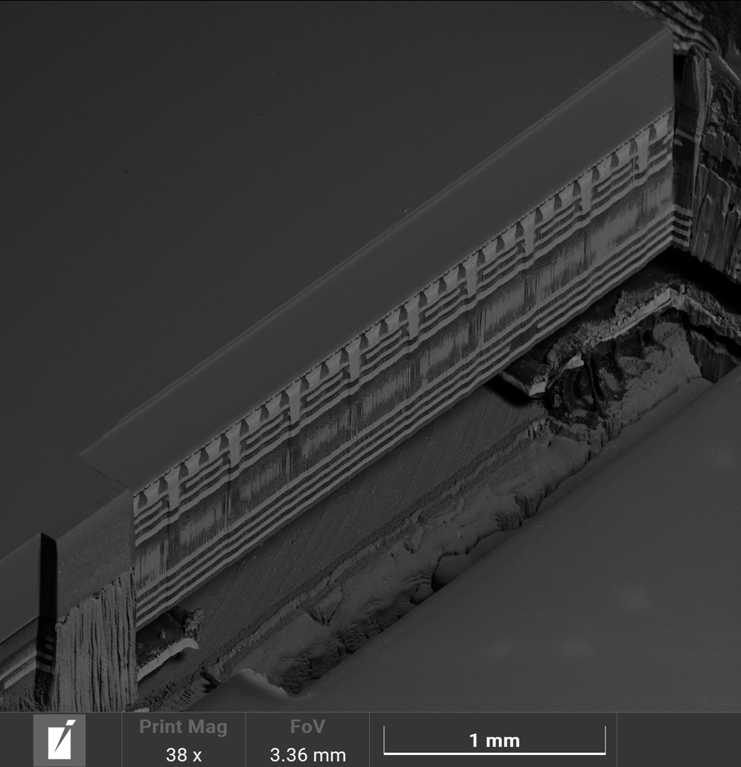
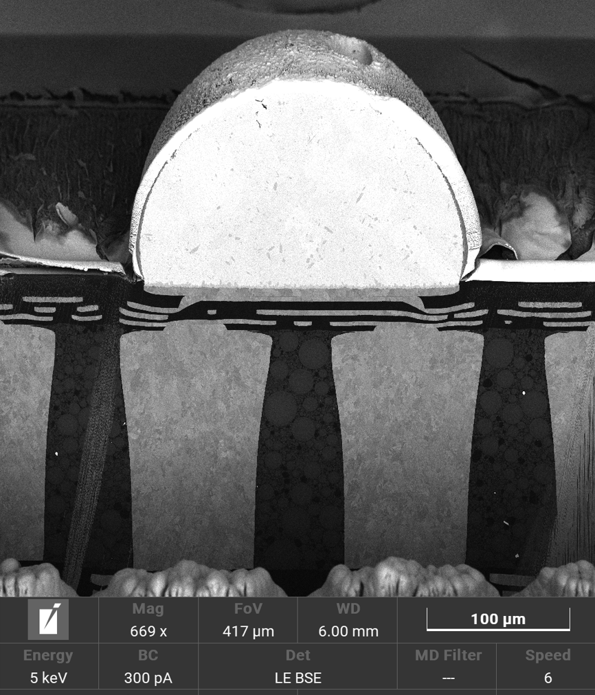
Deliver Deep, Artifact-Free Cross Sections
Achieve clean, reliable results on complex IC packages using Rocking Stage and TRUE X-sectioning.

Solve package-level failure challenges with Tescan SOLARIS X 2 Plasma FIB-SEM. Designed for today’s complex IC packaging, SOLARIS X 2 combines the Mistral™ Xe Plasma FIB column with Rocking Stage, TRUE X-sectioning, and the Triglav™ UHR SEM to deliver deep, clean cross-sections and precise end-pointing.