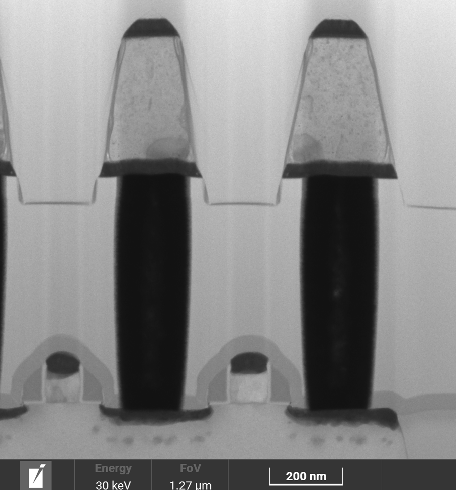
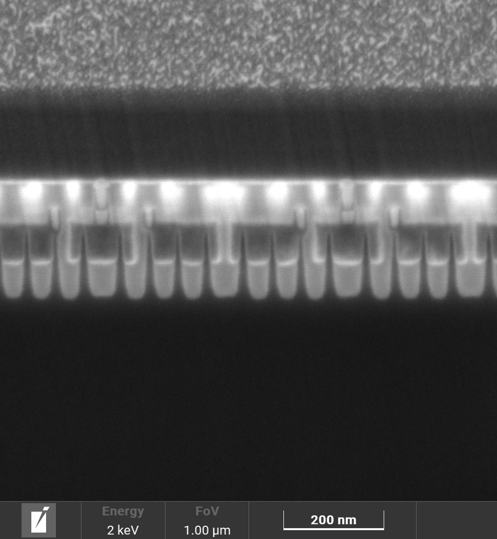
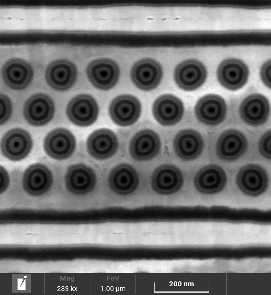
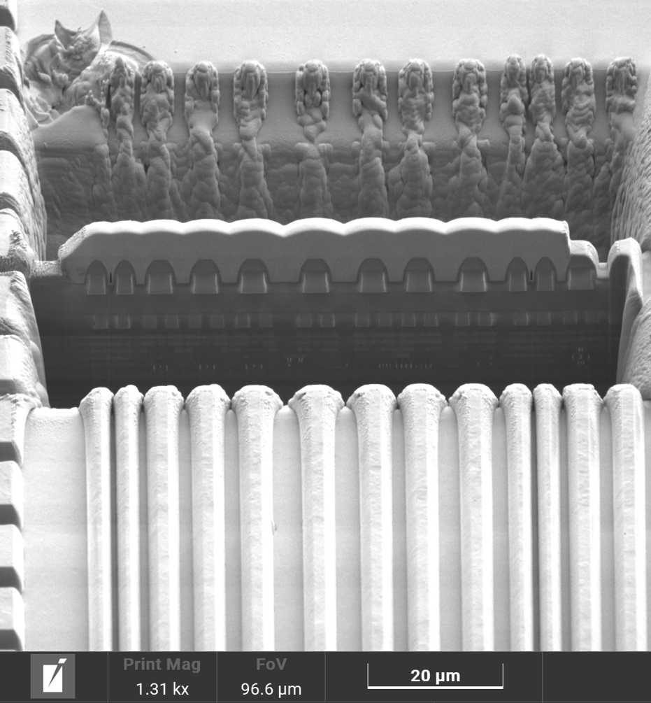
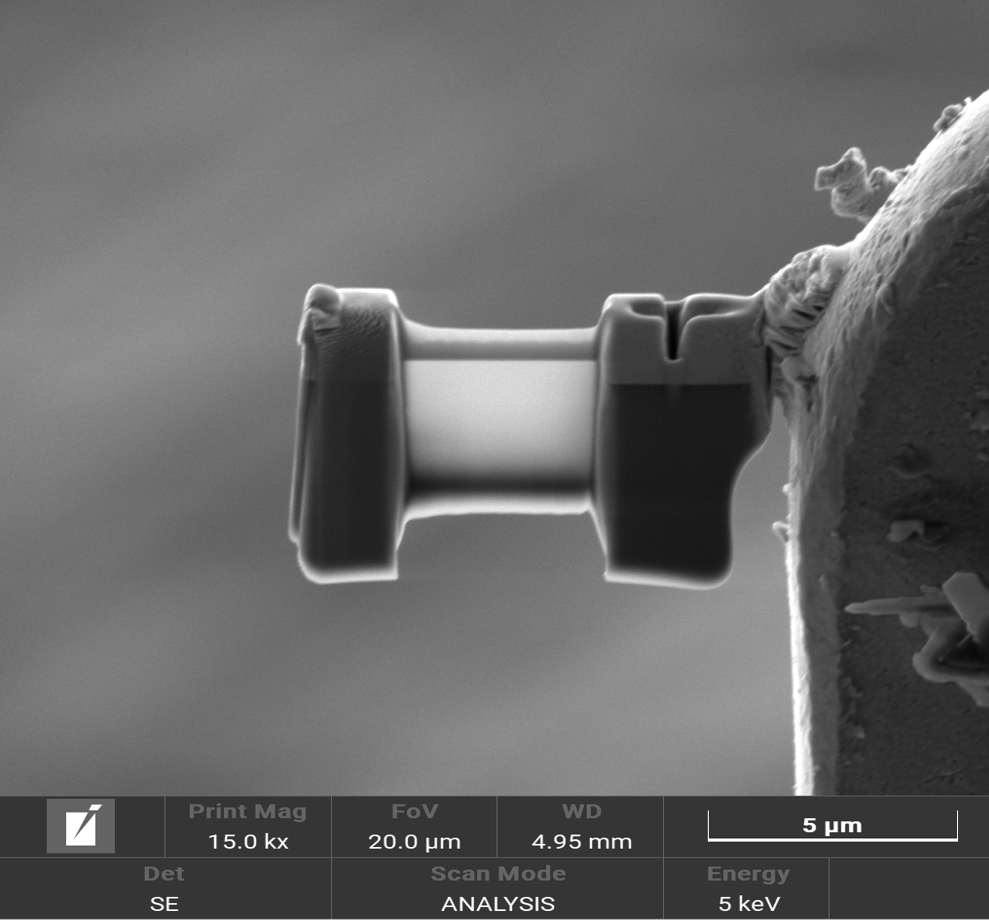
Produce Sub-100 nm TEM Lamellae in Under an Hour
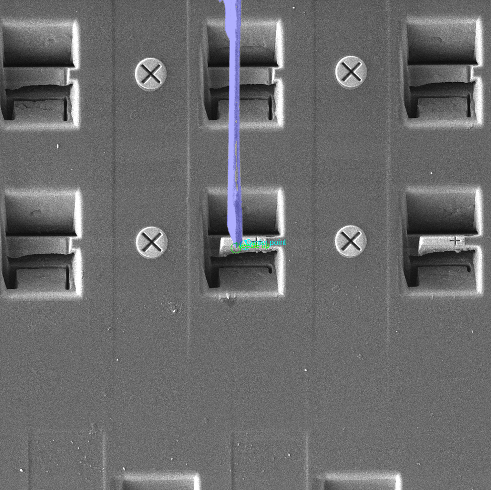
Automate the entire workflow, from trenching to lift-out and final polishing, with TEM AutoPrep™ Pro for fast, repeatable results.

Advance semiconductor TEM workflows with Tescan SOLARIS 2 Ga FIB-SEM. Purpose-built for failure analysis, R&D, and quality control, SOLARIS 2 integrates the Orage™ 2 Ga FIB column, Triglav™ UHR SEM, TEM AutoPrep™ Pro, and OptiLift™ nanomanipulator to deliver precise, fully automated TEM lamella preparation in under one hour.