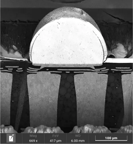
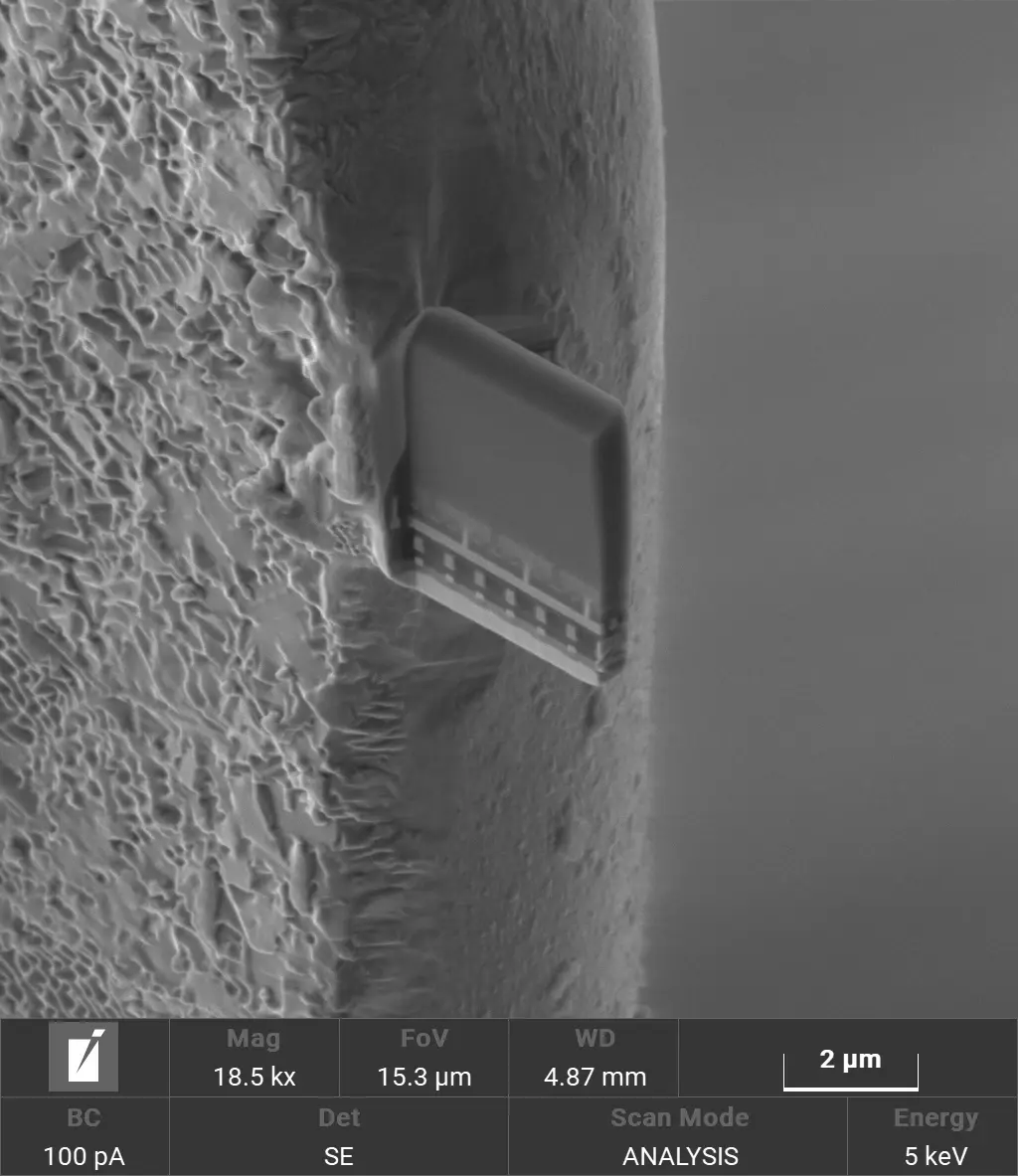
This is a title
Contextual advertising can be profitable. It can either pay for your hosting and maintenance costs for you website or it can pay for a lot more.
Gain deeper insights into the microstructure, composition, and performance of materials with Tescan AMBER X Plasma FIB-SEM. Designed for high-resolution 3D imaging and large-volume analysis, AMBER X enables precise cross-sectioning and reconstruction of complex materials, advancing research in energy storage, metals, ceramics, and nanomaterials.
Contextual advertising can be profitable. It can either pay for your hosting and maintenance costs for you website or it can pay for a lot more.
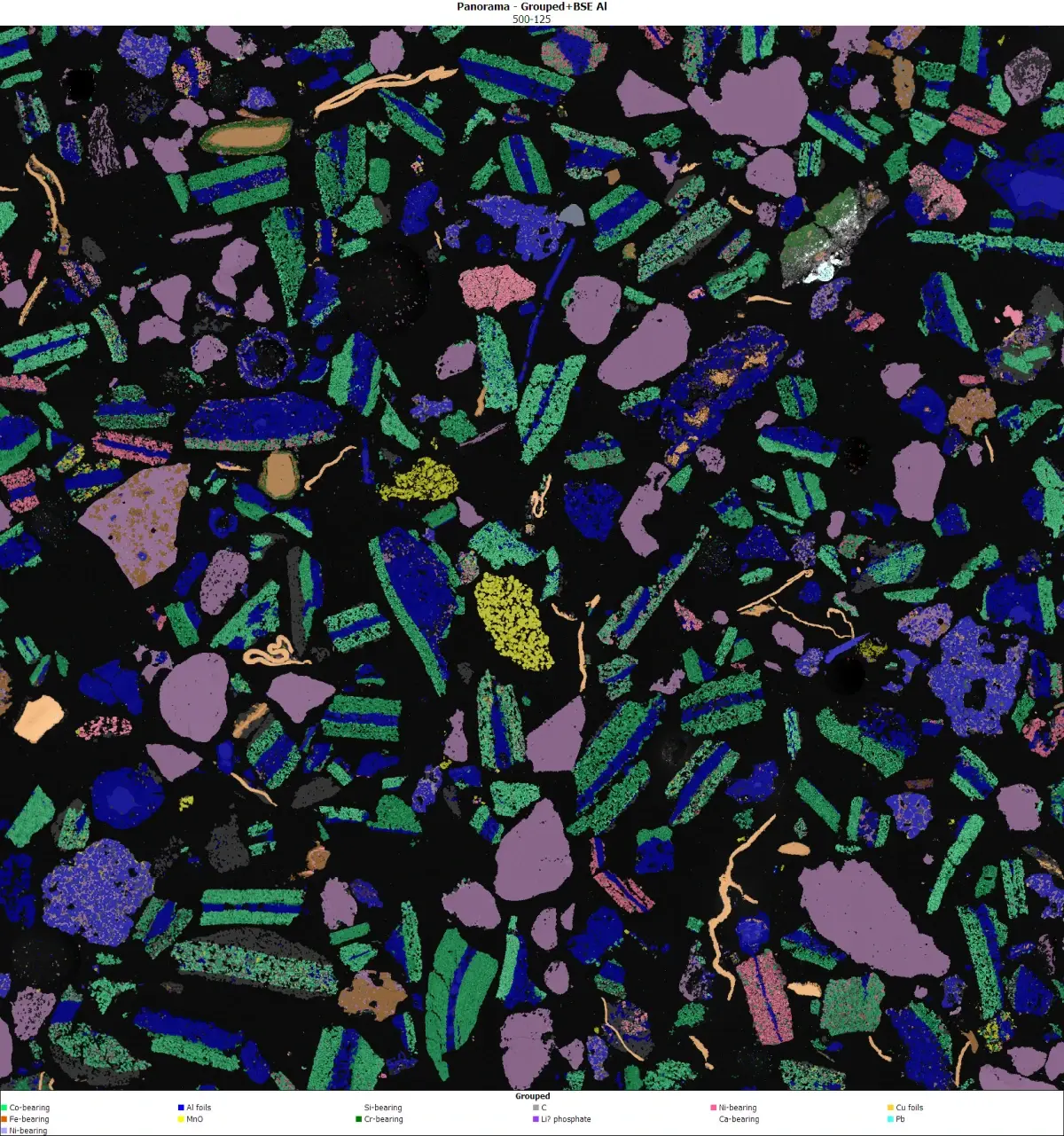
Its integrated control of FIB-SEM, EDS, EBSD, and advanced imaging tools ensures seamless operation, reducing user workload and increasing reproducibility. With AI-driven automation and real-time data visualization, Tescan Essence™ enhances efficiency, making even complex analyses faster and more accessible to both expert and novice users.
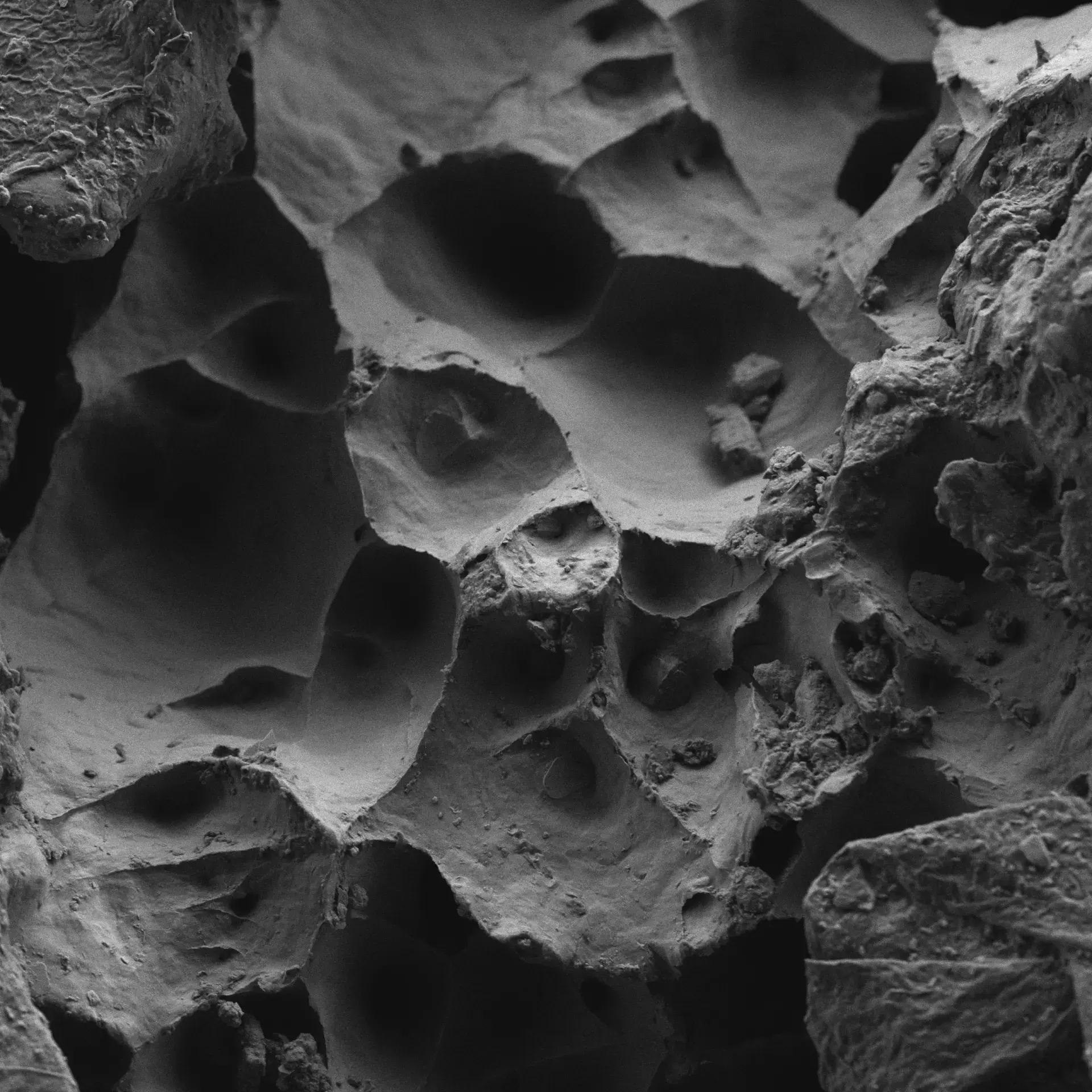
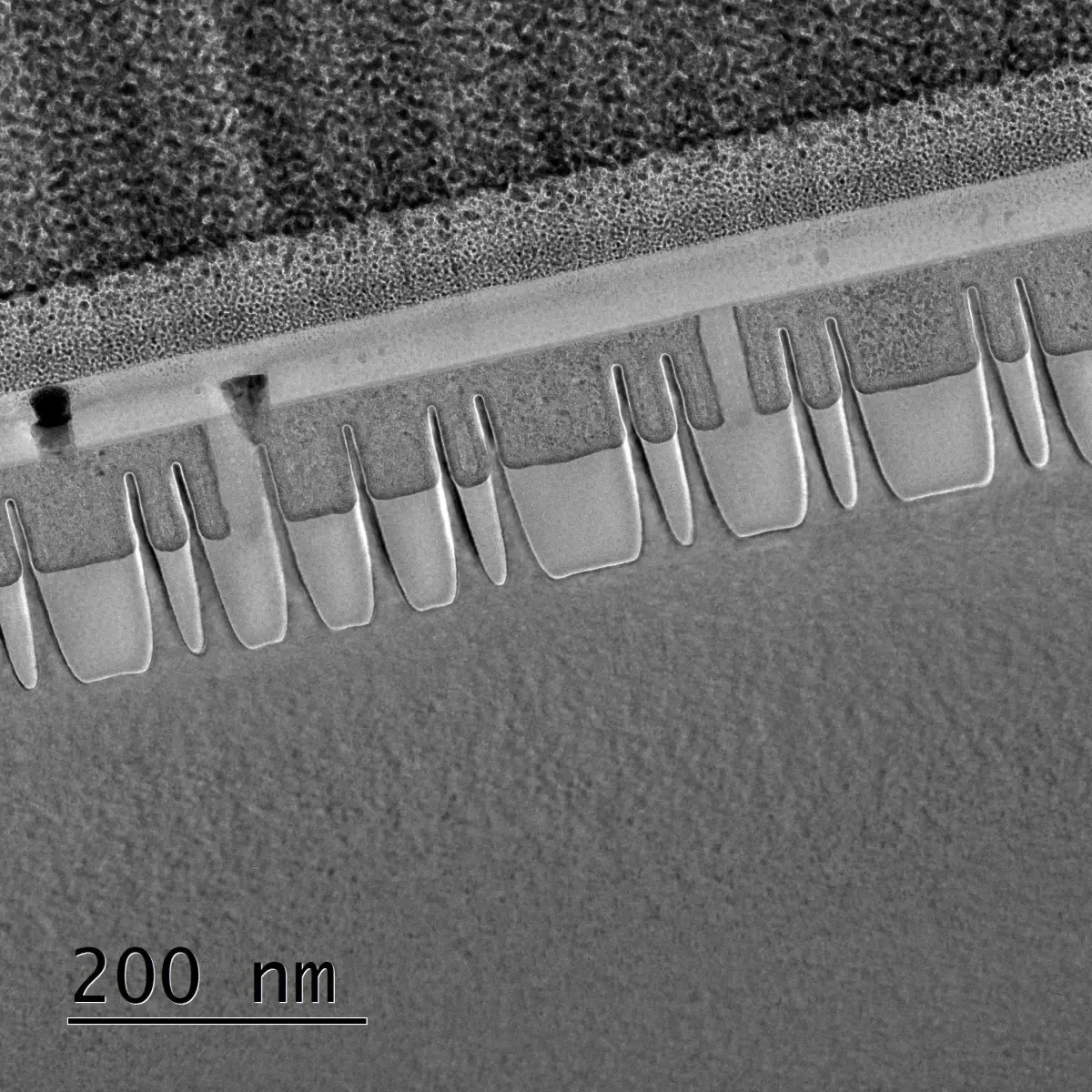
Tescan AMBER X with iFIB+™ control and real-time SE signal end pointing delivers precise Sub-20 nm node delayering. Achieve planar surfaces below 5 nm RMS roughness, maintain dielectric compatibility, and prepare contamination-free structures ready for in-situ nanoprobing and electrical failure analysis.
Advanced materials used in energy storage, aerospace, nanotechnology, and biomedical applications require in-depth structural insights. However, traditional imaging techniques often fall short when analyzing multi-phase structures, nanoscale defects, and buried interfaces.
Tescan’s FIB-SEM tomography workflow enables researchers to analyze materials at an unmatched resolution, revealing critical structural details that impact performance, durability, and failure mechanisms.
Targeted Material Selection
Identifying the region of interest with SEM and correlative imaging.
Precision Ion Beam Milling
Identifying the region of interest with SEM and correlative imaging.
3D Image Acquisition & Reconstruction
Identifying the region of interest with SEM and correlative imaging.
Advanced materials used in energy storage, aerospace, nanotechnology, and biomedical applications require in-depth structural insights. However, traditional imaging techniques often fall short when analyzing multi-phase structures, nanoscale defects, and buried interfaces.
This is more than information; it's an advantage. We've compiled our technical whitepapers, detailed product flyers, and on-demand webinars to provide you with the knowledge that makes a real difference. Sign up now to access the insights you need to make an impact.
|
SEM
|
Resolution
|
20 eV - 30 keV
|
|---|---|---|
|
Landing energy
|
0.6 nm @ 15 keV
1.0 nm @ 1 keV |
|
|
STEM
|
Resolution @ 30 keV
|
0.7 nm
|
|
FIB preparation
process |
Max material removal
|
100 nA
|
|
Optimal final polish
|
2 kV
|
|
SEM
|
|---|
|
Resolution
|
20 eV - 30 keV
|
|
Landing energy
|
0.6 nm @ 15 keV
1.0 nm @ 1 keV |
|
STEM
|
|---|
|
Resolution @ 30 keV
|
0.7 nm
|
|
FIB preparation
process |
|---|
|
Max material removal
|
100 nA
|
|
Optimal final polish
|
2 kV
|
Tescan Brno
Libušina tř. 21
623 00 Brno - Kohoutovice
Czech Republic
+420 530 353 411
info@Tescan.com